Review
The Five Classic Components
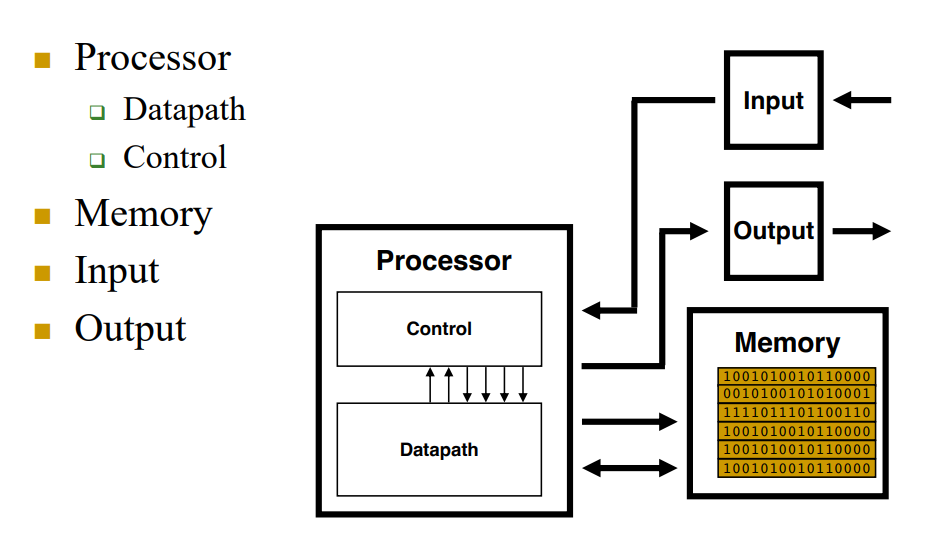
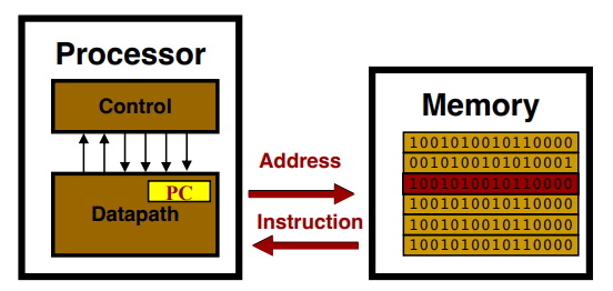
Processor Operation
- Processor fetches instruction from memory. (by. memory address)
- Processor executes machine language instruction.
- Perform calculation
- Read/Write data - Repeat with "next" instruction: 4 bytes away from current PC
Steps in Processor Design
- Analyze instruction set; get datapath requirements.
- Select datapath components and establish clock methodology.
- Assemble datapath that meets requirements.
- Determine control signal values for each instruction.
- Assemble control logic to generate control signals.
Processor Implementation Styles
- Single Cycle: 1 clock cycle = 1 instruction 수행
- Multi-Cycle: Perform 1 step in each clock cycle.
- 5 steps: fetch --> decode --> ALU --> access --> update - Pipelined: Perform 1 step/instruction in each clock cycle.
"MIPS Lite" - a pedagoical example
- Memory access: lw, sw
- Arithmetic/Logical: add, sub, and, or, slt(if A<B, $s0 = 1)
- Branch/Jump: beq, j
Review
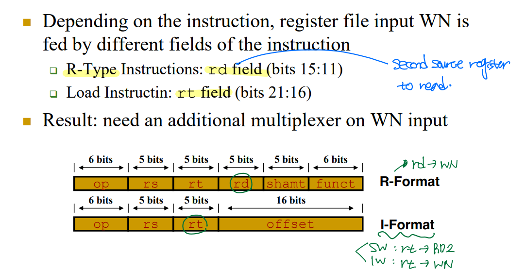
MIPS Instruction Format

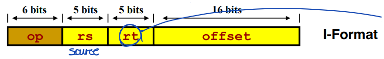
beq  $rs, $rt, offset

lw   $rs, offset($rt)     # $rt: write
sw   $rs, offset($rt)     # $rt: read
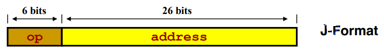
jump
MIPS Instruction Subset
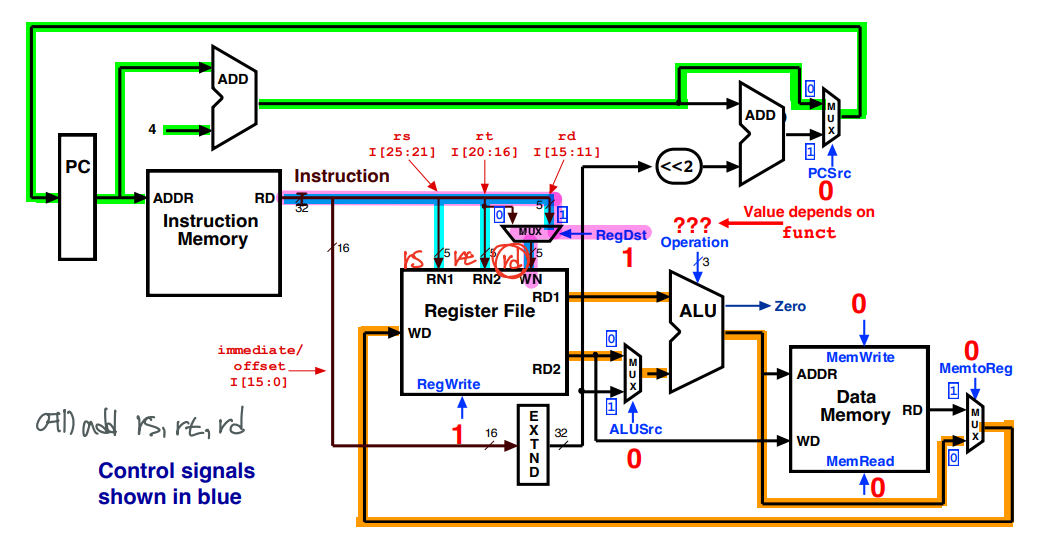
▶ Arithmetic/Logical Instructions:
# R-Format

add  $s0, $s1, $s2
sub  $s0, $s1, $s2
and  $s0, $s1, $s2
or   $s0, $s1, $s2
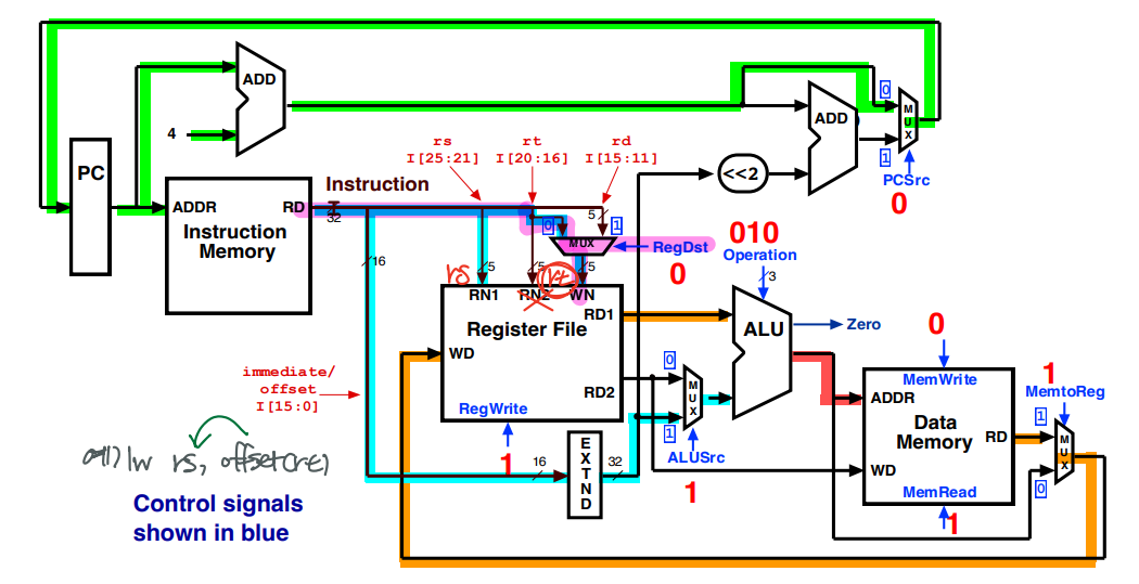
▶ Data Transfer Instructions:
# I-Format

lw  $s0, offset($s1)
sw  $s2, offset($s3)
▶ Branch:
# I-Format
beq  $s0, $s1, offset

# J-Format
j    address
MIPS Instruction Execution
- Fetch instruction from memory. (by. PC)
- Decode instruction, read register values. (Format 확인하고, ...)
- If necessary, perform ALU operation.
- If load or store, do memory access.
- Write results back to register file and increment PC.
Register Transfers for the MIPS Subset
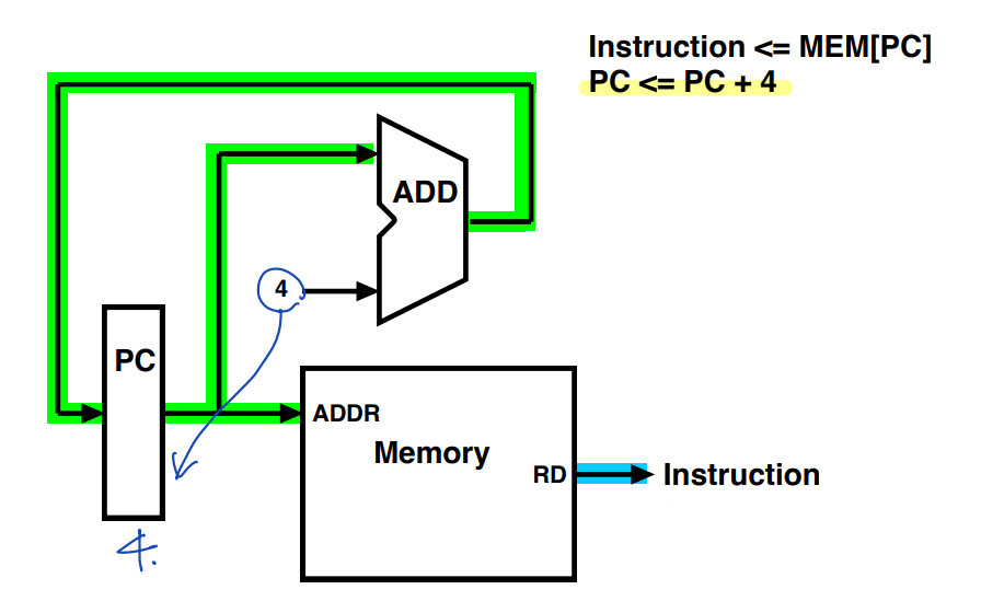
- Instruction Fetch: Instruction <= MEM[PC]
- Instruction Execution
# R-Format
add R[rd] <= R[rs] + R[rt];
sub R[rd] <= R[rs] - R[rt];
and R[rd] <= R[rs] & R[rt];
or R[rd] <= R[rs] | R[rt];
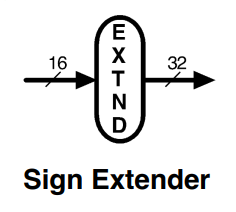
# I-format: sign extension
# Load, Store
lw R[rt] <= MEM[R[rs] + sign_extend(offset)]; # lw: memory --> register (read, write)
sw MEM[R[rs] + sign_extend(offset)] <= R[rt]; # sw: register --> memory (read, read)
# Branch
beq if(R[rs] == R[rt]), PC <= PC+4 + sign_extended(offset<<2); else, PC <= PC+4
# J-Format
j PC <= upper(PC)@(address<<2)
1. Instruction Set Requirements
▶ Memory
- Read instructions
- Read/Write data
▶ Registers (5-bit, 32 registers)
- R-format: Read from rs, rt, Write to rd.
- I-format:
- lw: Read from rs, Write to rd.
- sw: Read from rs, rd.
- beq: Read from rs, rd. - J-format: j
2-1. Choose Datapath Components
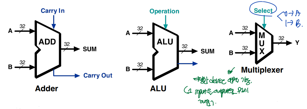
1) Datapath Combinational Components
- Adder
- ALU: 어떤 연산을 할 지 결정한다.
- MUX (Multiplexer)
- Sign-Extender
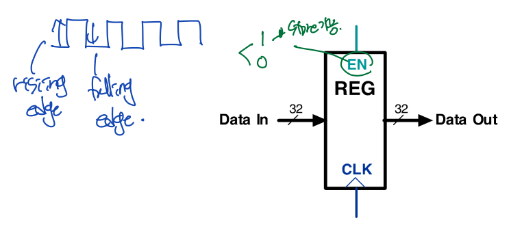
2-1) Datapath Storage Components - Registers
- Registers store multiple bit values.
- New values loaded on clock edge (clock rising edge에서 store the data) when EN(enable bit) asserted.
2-2) Datapath Storage Components - Idealized Memory
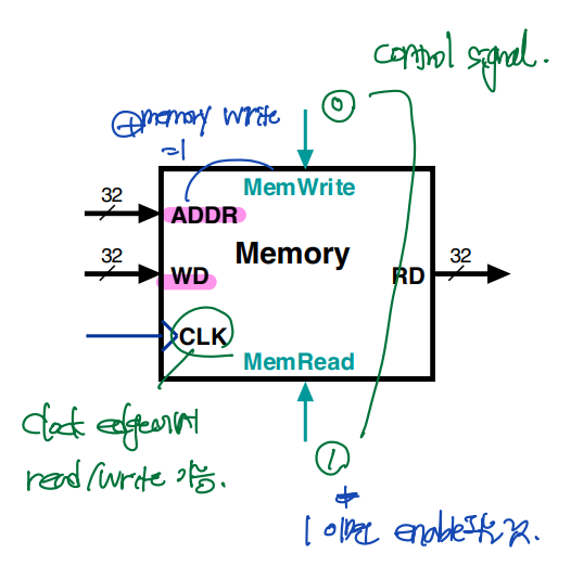
▶ Data Read:
- Place address on ADDR.
- MemRead = 1;
- Data available on RD. (after memory access time)
▶ Data Write:
- Place address on ADDR.
- Place data input on WD.
- MemWrite = 1;
- Data written on clock edge.
2-3) Datapath Storage Components - Register File
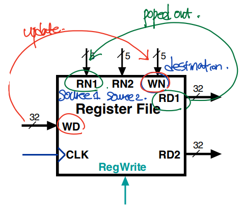
▷ Register file: 32-bit registers
▶ Read:
- Assert register number RN1, RN2.
- Read output RD1, RD2. (after access time)
▶ Write:
- Assert register number WN.
- Assert value on WD. (WD: writing input)
- Assert RegWrite.
- Value loaded on clock edge.
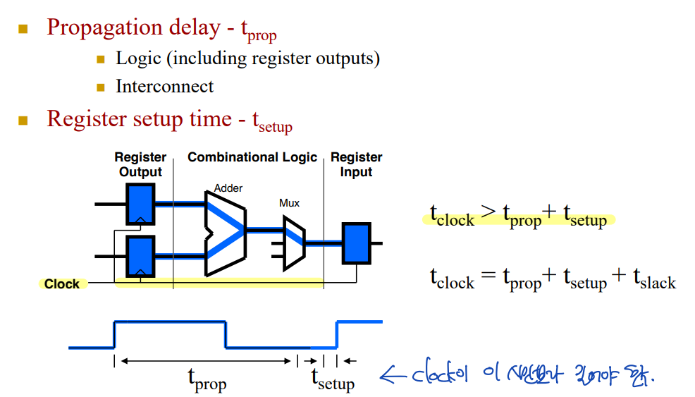
2-2. Choose Clocking Methodology
--> Author's choice: Clock rising-edge에서 동작한다.
Edge-Triggered Clocking
▶ Controls sequential circuit operation
- 1st clock edge: Register outputs change.
- Combinational logic determines "next state".
- 2nd clock edge: Storage elements store new state.
3. Assemble Datapath
- Fetch instruction from memory.
- Decode instruction, read register values.
- If necessary, perfrom an ALU operation.
- If memory address, perform load/store. (lw: read/write, sw: read/read)
- Write results back to register file and increment PC.
cf) PC는 이전에 4 byte만큼 incremented되어 있음!
Datapath for Instruction Fetch
: PC 값에 따라 instruction fetch
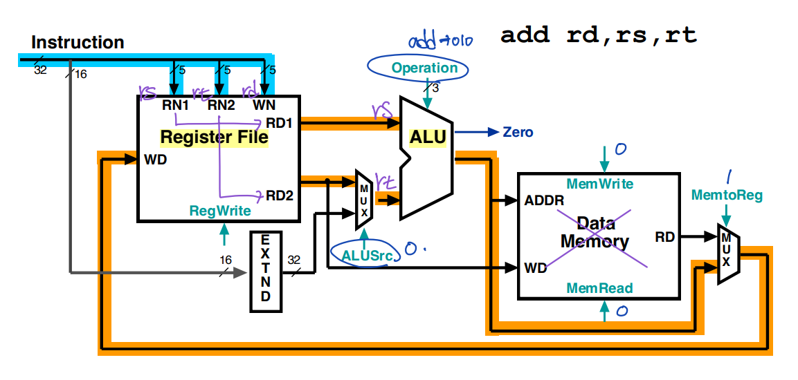
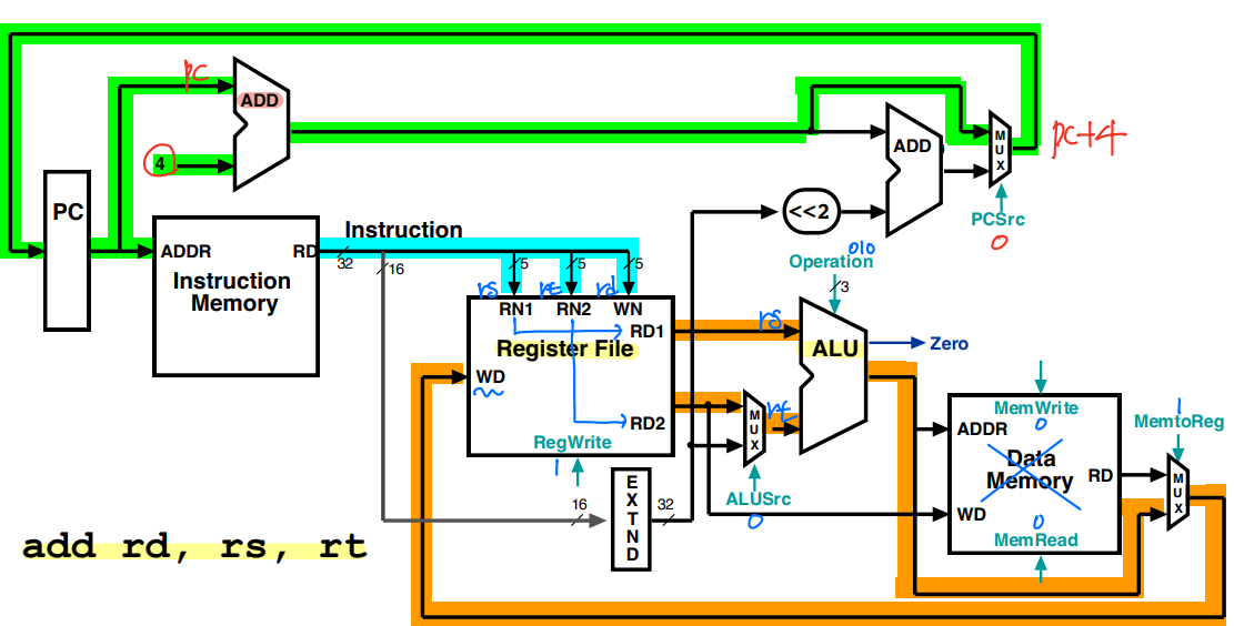
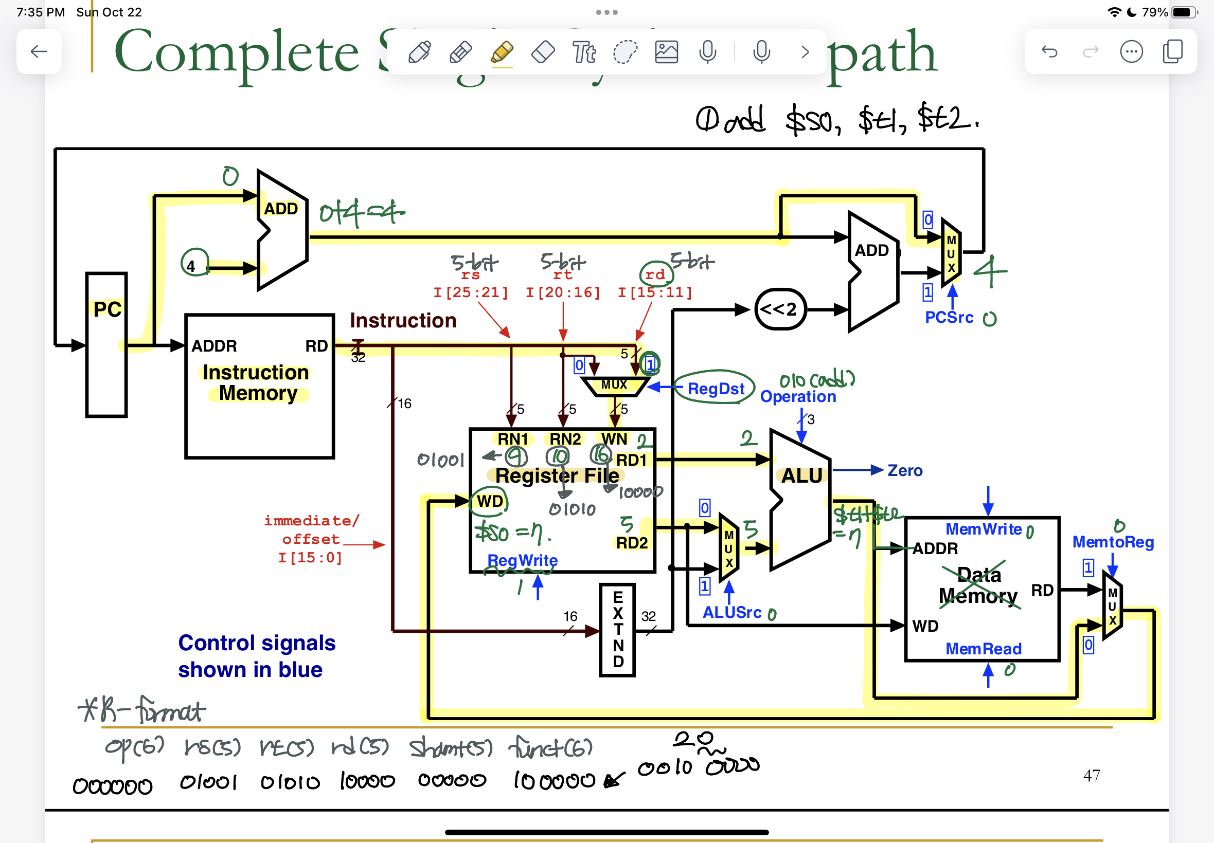
1) Datapath for R-Type Instructions
add $s0, $t1, $t2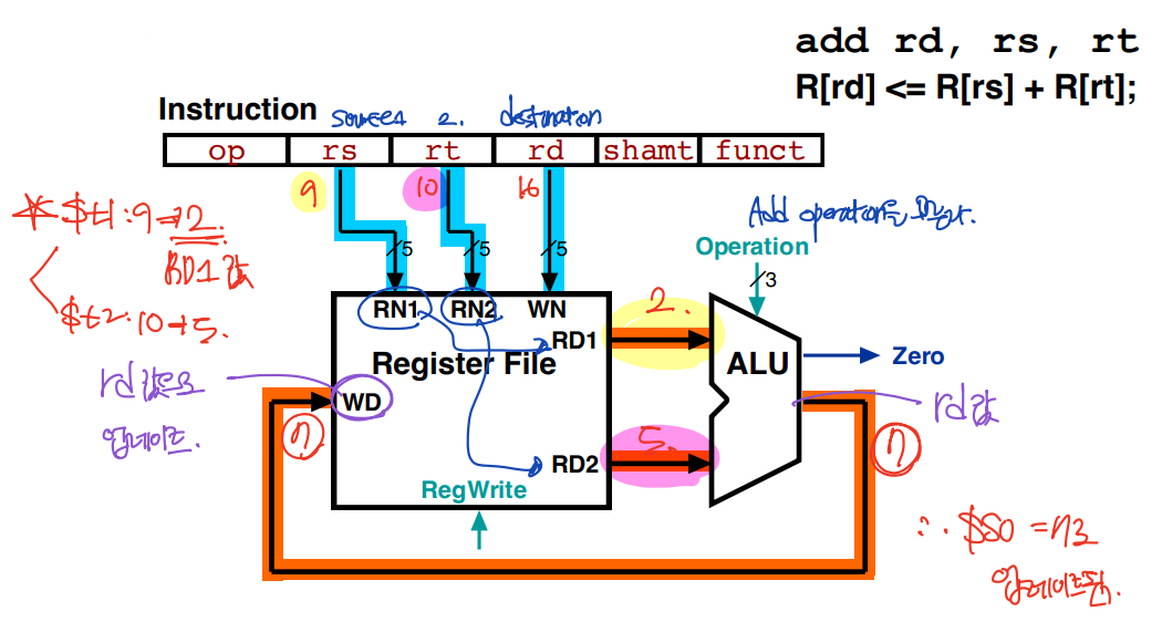
1. Register File
- RN1 = 9 ($t1 번호) --> RD1 = 2 ($t1 값)
- RN2 = 0 ($t2 번호) --> RD2 = 5 ($t2 값)
- WN = 16 ($s0 번호)
2. ALU
- Operation = 010 (add 연산)
- WD = 7 (연산 결과, write)
--> $s0 = 7로 업데이트 된다.
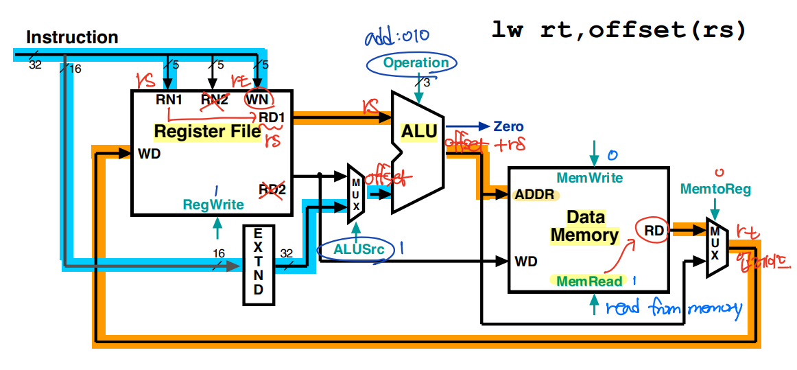
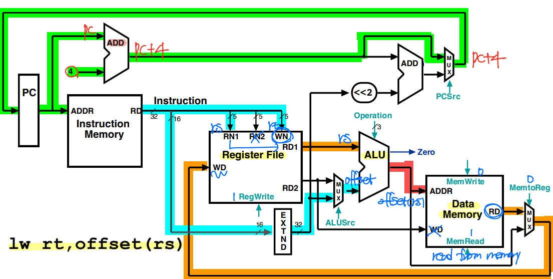
2) Datapath for Load/Store Instructions
lw rt, offset(rs)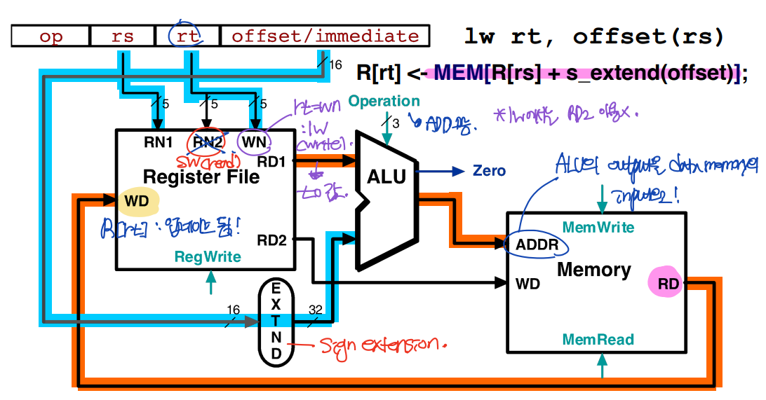
1. Register File
- RN1 = rs --> RD1
- WN = rt (Load된 데이터를 저장할 레지스터; write)
2. ALU
- input으로 RD1, offset 값이 들어가서 add. (Operation = 010)
- output을 ADDR에 저장한다.
3. Memory
: RD 값이 Register File의 WD로 흘러가서, R[rt] 값이 업데이트 된다. (레지스터에 write)
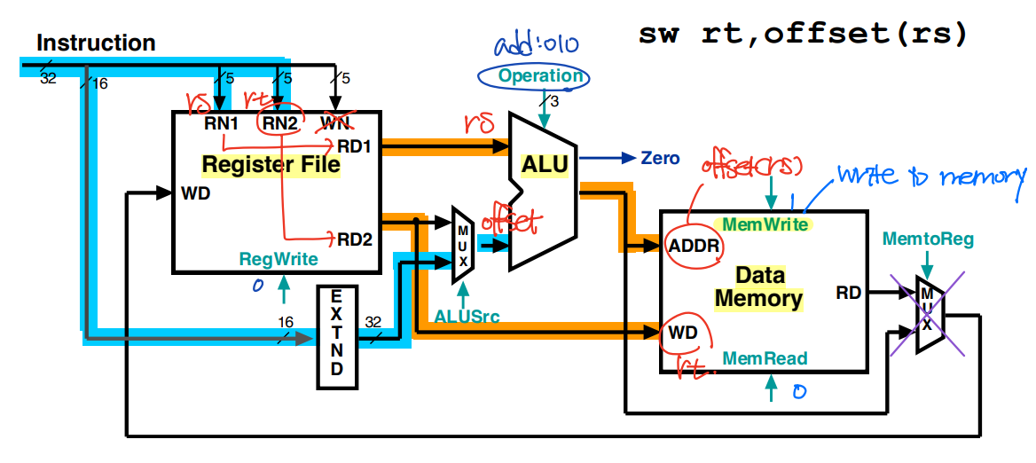
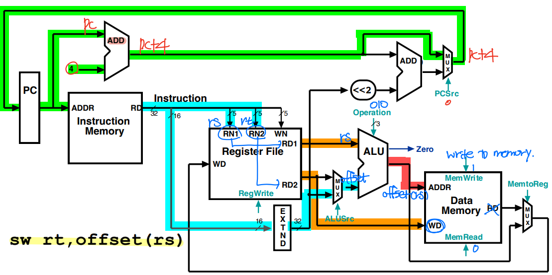
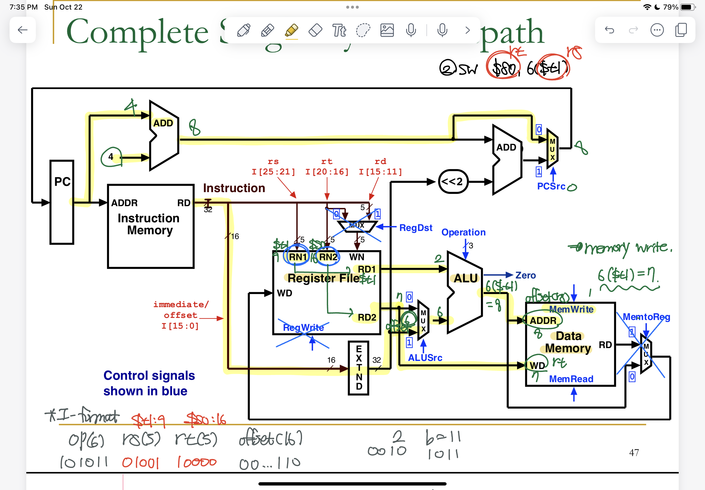
sw rt, offset(rs)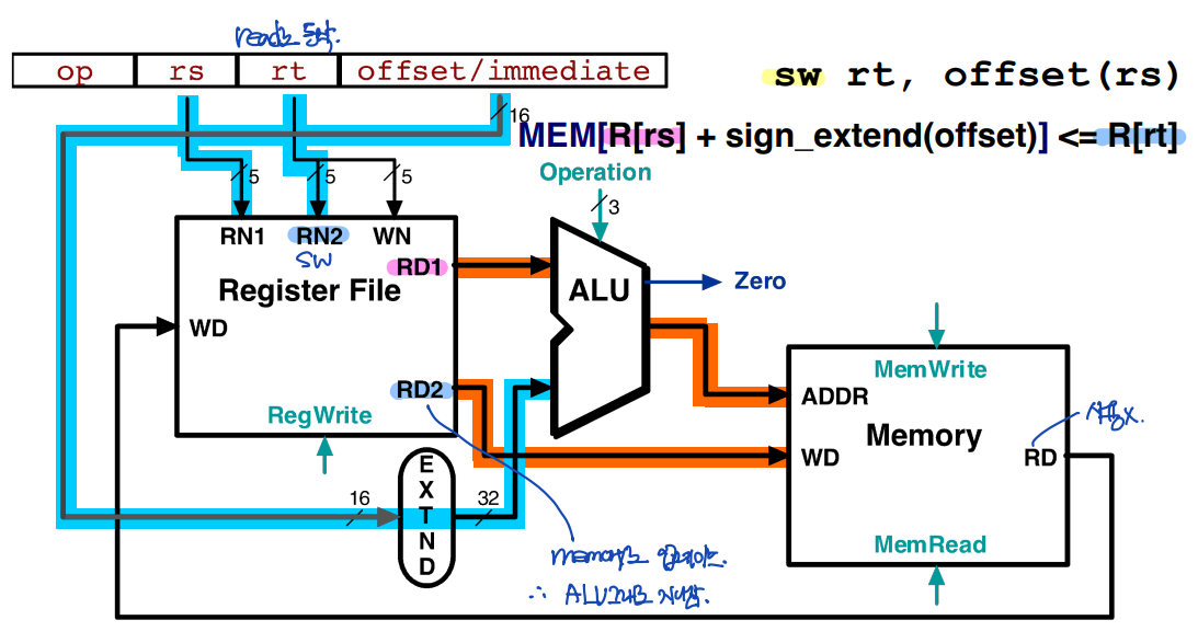
1. Register File
- RN1 = rs --> RD1
- RN2 = rt (sw: read/read) --> RD2
2. ALU
- input으로 RD1, offset 값이 들어가서 add. (Operation = 010)
- output을 ADDR에 저장한다.
3. Memory
- ADDR = ALU 계산 결과
- WD = RD2 값 (메모리에 wirte)
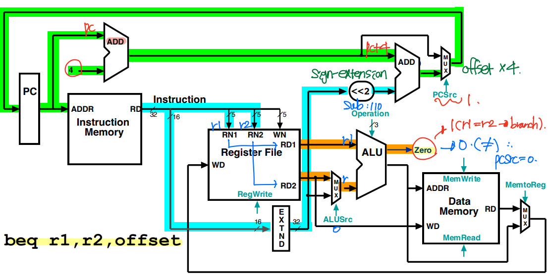
3) Datapath for Branch Instructions
beq rs, rt, offset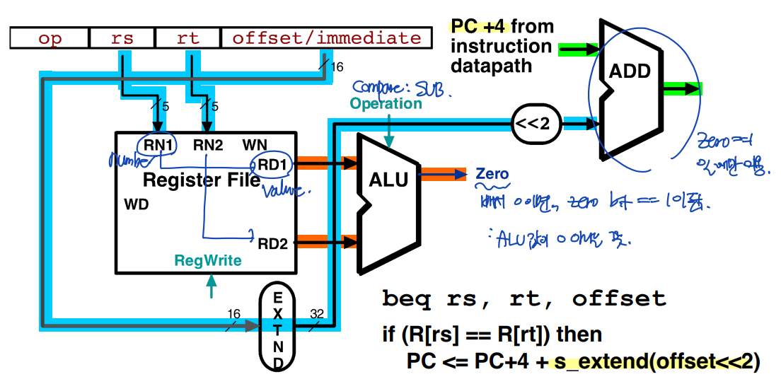
1. Register File
- RN1 = rs --> RD1
- RN2 = rt --> RD2
2. ALU
- input으로 RD1, RD2 들어가서 sub(비교 연산). (Operation = 110)
- (RD1 - RD2 = 0)이면, Zero bit = 1;
3. ADD
: Zero bit == 1일 때, 즉 RD1 == RD2 일 때만 동작한다. (branch if equal)
- offset << 2 (offset * 4): sign-extension
- PC + 4
--> Putting it all together...
- Goal: merge datapath for each function!
- Add MUX to steer data needed!
Combined Datapath: R-Type and Load/Store Instructions
1) Combined Datapath: Executing R-Type Instruction
2) Combined Datapath: Executing a Load Instruction
3) Combined Datapath: Executing a Store Instruction
Complete Single-Cycle Datapath
1) Complete Datapath: Executing ADD
2) Complete Datapath: Executing Load
3) Complete Datapath: Executing Store
4) Complete Datapath: Executing Branch
Refining the Complete Datapath
Complete Single-Cycle Datapath
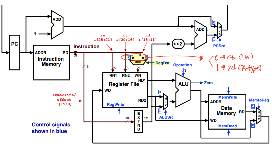
1) Control Signals: R-format Instruction
2) Control Signals: lw Instruction
3) Control Signals: sw Instruction

4) Control Signals: beq Instruction
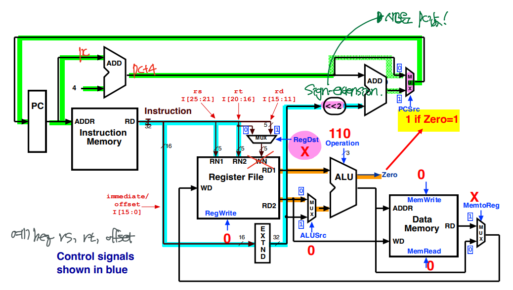
- if (R[rs] == R[rt]), then PC <= PC+4 + sign_extended(offset<<2);
즉, PC가 이미 (PC+4)를 하는 adder의 결과를 타고 가다가, beq condition을 만족할 때 한번 더 adder를 통해 더해지는 구조이기 때문에, (PC+4)가 이미 저장되어 있는 상황에서, 추가로 (offset<<2)만큼 더해져서, branch할 주소를 결정하게 된다.
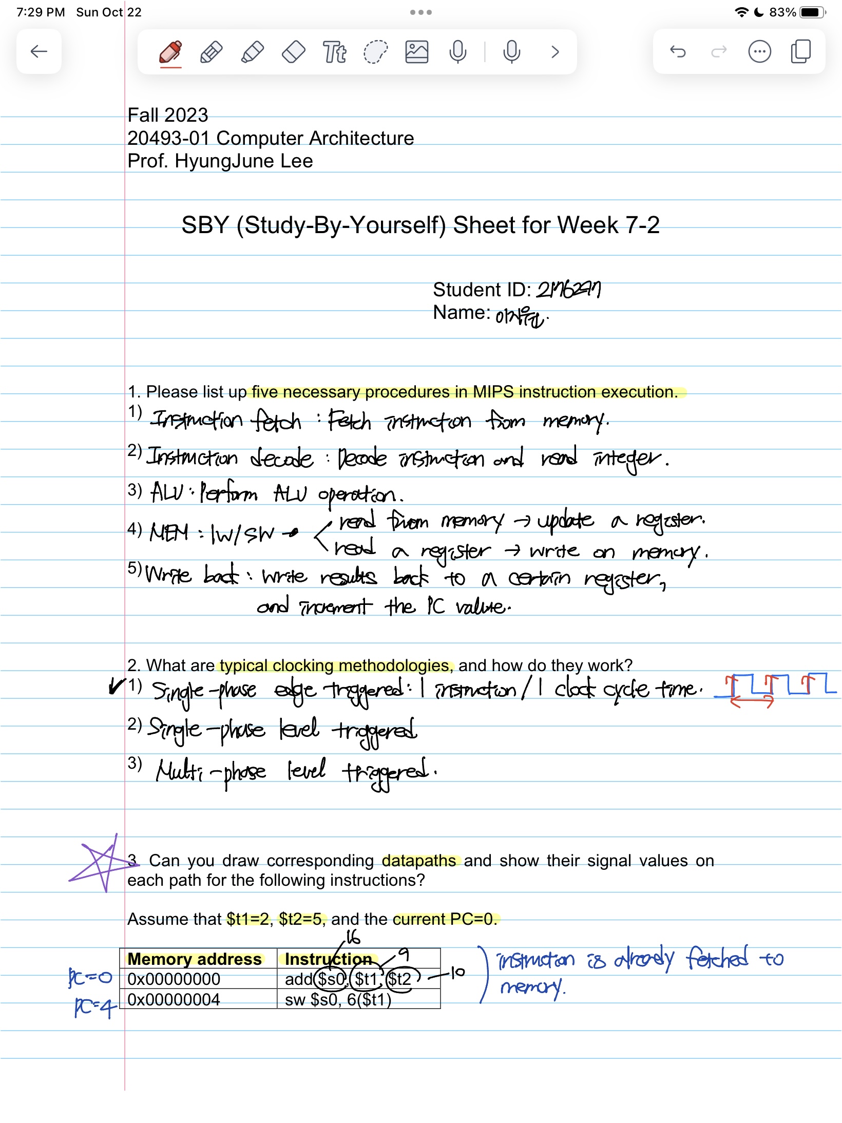
SBY 7-2
'Computer Architecture > 컴퓨터구조[01]' 카테고리의 다른 글
| [컴퓨터구조] 1101 (0) | 2023.11.05 |
|---|---|
| [컴퓨터구조] 1030 (1) | 2023.11.02 |
| [컴퓨터구조] 3. Arithmetic for Computers (4) (0) | 2023.10.22 |
| [컴퓨터구조] 3. Arithmetic for Computers (3) (0) | 2023.10.22 |
| 2. 컴퓨터 언어 (0) | 2023.10.17 |


